FPGA-8-Bit-Computer
Project Description and Source Code
View the Project on GitHub jerrycampbellus/FPGA-8-Bit-Computer
FPGA 8 Bit Computer Based on Ben Eater's Discrete Component Design and Implementation
Background
Like many people who found Ben Eater's 8-bit computer project on YouTube, the series was highly informative and engaging, and it inspired me to take on this project. Ben's approach to building his 8-bit computer and his logical, linear, and realistic style of explaining concepts have motivated many to understand computers and what makes them work. I encourage you to review his website for more information or purchase kits to build the computer.
Although I did not build his design using discrete components, I did think there would be value in creating a working implementation with an FPGA, field-programmable gate array. There are several notable examples of using an FPGA to realize full computers or individual components such as the CPU, video card, and I/O devices. This project designs and implements the same elements in Ben's initial design but uses an FPGA development card instead of breadboards and ICs. An exciting challenge and complementary project to the original project.
Goals
When I considered the goals for my project, I wanted to keep the outcome closely aligned to the outputs from Ben's original project. I wanted to develop an 8-bit Touring complete computer with a limited instruction set as an instructional and, hopefully, an inspirational project for others interested in FPGA design and 8 -bit computer architecture. I wanted to leverage the capability of most FPGA design boards and incorporate inputs and outputs accessible from most manufacturers. Finally, I tried to make the design portable between FPGA manufacturers and development boards, so I built the solution without using softcore intellectual property. All solution elements are written in Verilog and can be customized using an appropriate, manufacture-specific, top-level module to specify a clock, inputs, and outputs. Using these principles, I developed the following list of goals:
- One-to-one mapping between the original component design and the FPGA design
- Leverage development board-specific clocks, inputs (switches and buttons), and outputs (LEDs and HEX segments)
- Develop all modules using portable Verilog code without the use of Soft IP
- Utilize FPGA design, synthesis, placement and routing, timing analysis, and simulation tools provided by commercial FPGA manufacturers
The realization approach for each module took one of two paths. Either the module was defined using discrete IC models, or I created a pure Verilog definition. In the former case, I made a schematic file using primary logic gates, and in the latter case, I used design patterns from FPGA reference material. I created the Verilog source code and top-level constraint files for the Terasic FPGA DE10-Lite development board, utilizing a MAX10 FPGA from Alterra. The code repository contains the source files and the project archives from Altera's Quartus Prime software.
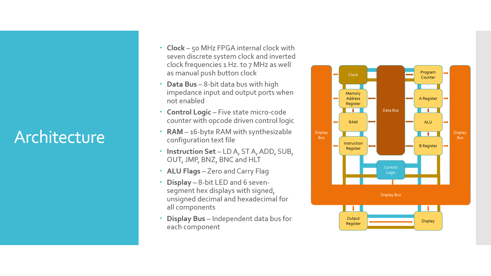
Architecture and Approach
The following represents the components in this project. Each component was developed, unit tested, then integrated to produce the final working system. Each of the components were implemented using either Verilog or built up through schematics entry.